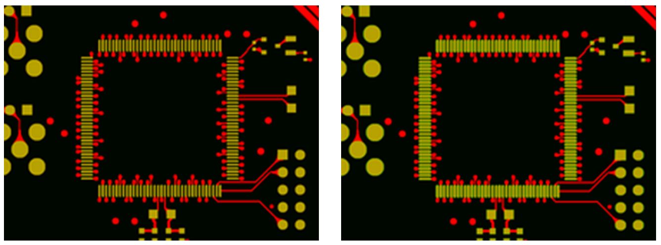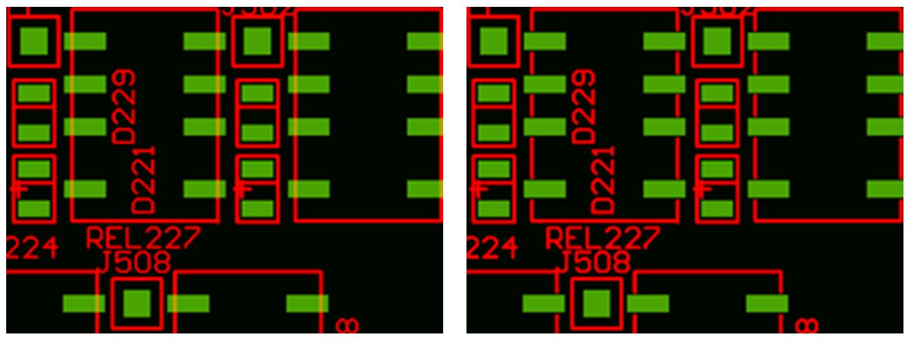

To prevent problems in PCB production and, mainly, in PCB assembly, solder mask should overhang the pads in adjacent layers (top and bottom) to a certain degree. Design systems, depending on their settings, mostly generate this overhang incorrectly, resulting in avoidable complications.
Therefore, we recommend generating solder mask pad size as 1:1 with solder pads. We then take care of this issue while processing your PCB production data in an automated manner.
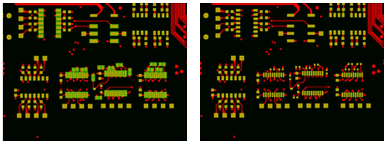
If the width of a gap between SMD pads in the artwork is below 200µm, we are technologically unable to achieve the bridge in the solder mask. The smallest bridge width is at least 120µm.