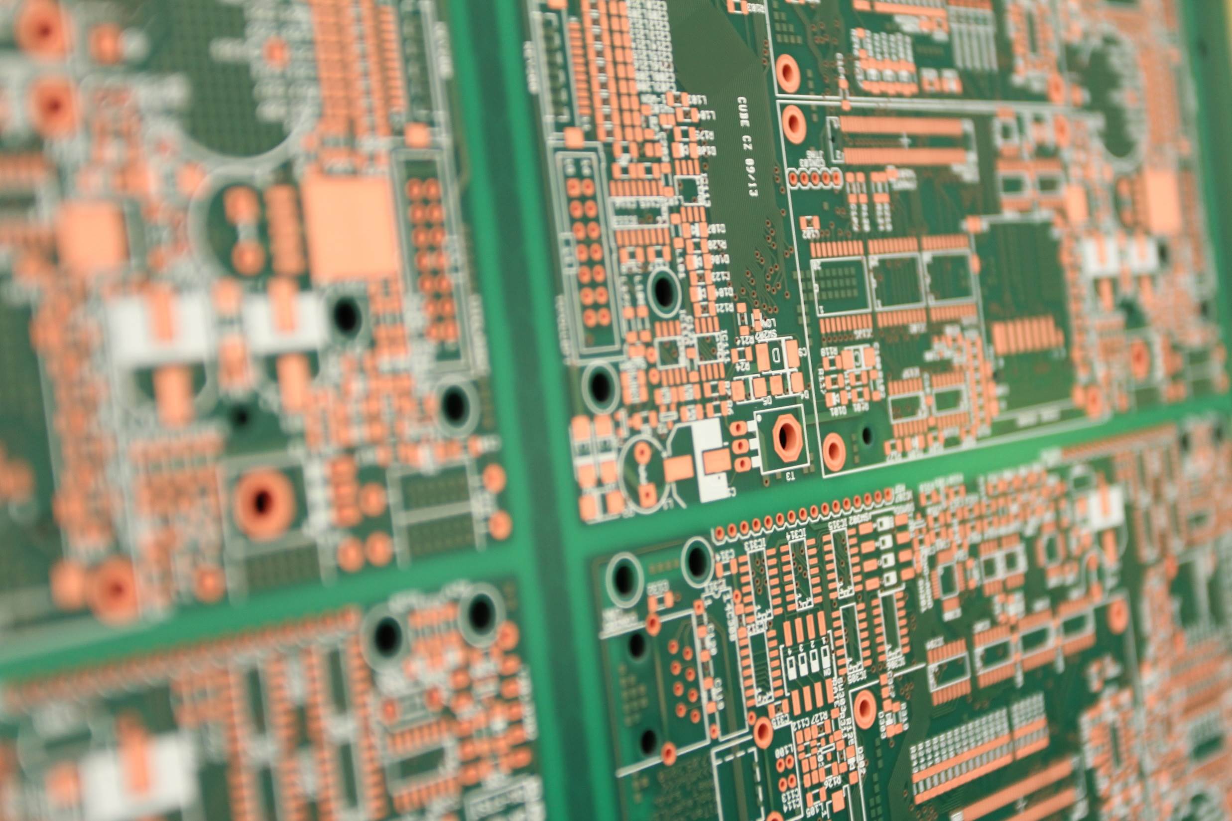
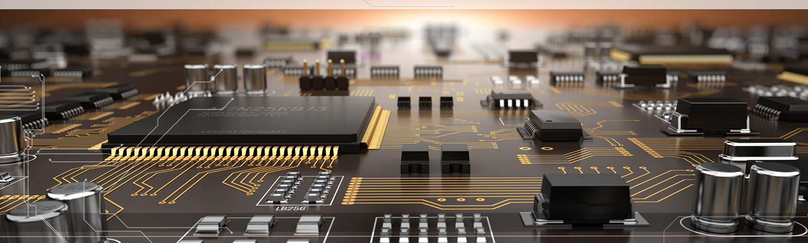
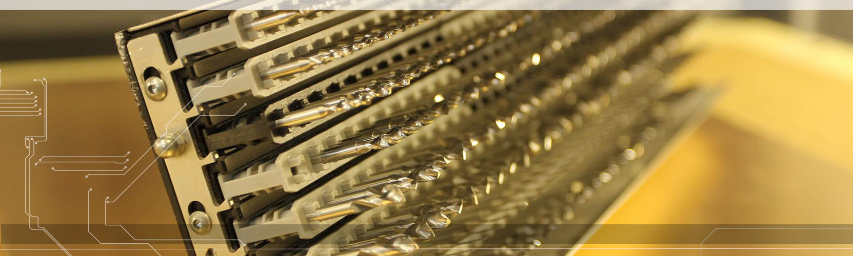
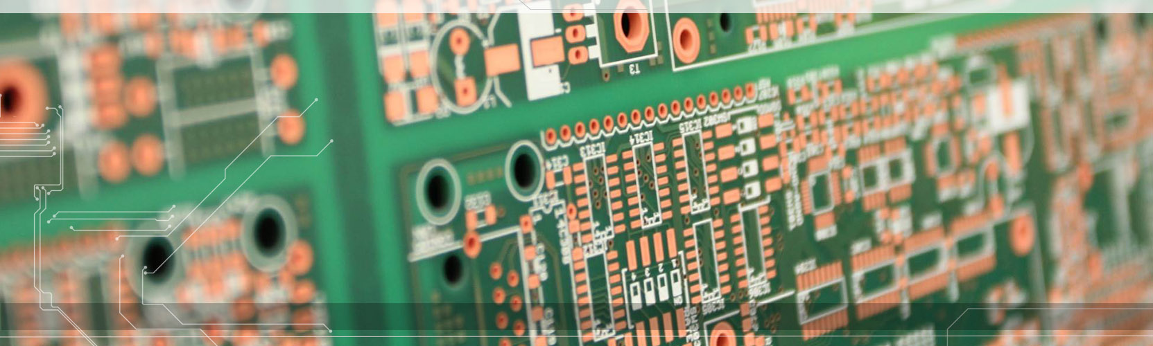
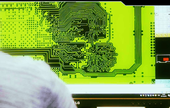
• One of the leadings czech PCB manufacturer
    with more than 30 years tradition
  • One of the leadings czech PCB manufacturer
    with more than 30 years tradition
  • One of the leadings czech PCB manufacturer
    with more than 30 years tradition
  • Most demanding technologies
    30 years tradition of PCB production
  • One of the leadings czech PCB manufacturer
    with more than 30 years tradition
  • One of the leadings czech PCB manufacturer
    with more than 30 years tradition
  • Most demanding technologies
    30 years tradition of PCB production
  • Most demanding technologies
    30 years tradition of PCB production
  • Most demanding technologies
    30 years tradition of PCB production
  • Most demanding technologies
    30 years tradition of PCB production

QUALITY INSPECTION – TESTING

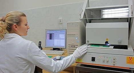
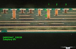
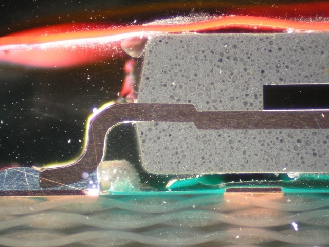
PCB Surface X-Ray Inspection

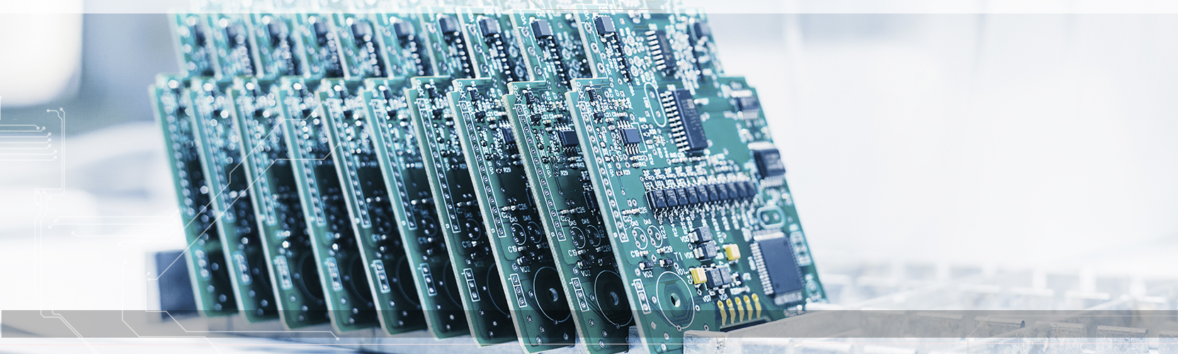
We have equipment for accurate, fast measurement of each final printed circuit board finish material thickness. We can measure separate thickness of nickel (Ni), chemical gold (Au), as well as immersion tin (Sn). We take such measurements routinely using sample boards from each delivery batch. The measurements result in a test report that includes measurement evaluation.

Method of Measurement – X-ray fluorescence

Fluorescent X-rays are emitted in a photo effect process. The principle of the process lies in an interaction between photons and the atom outer shell energy, Eo. The Energy Dispersive X-ray Fluorescence method (ED-XRF) is one of the simplest, most accurate, and most economical analytical techniques to determine chemical makeup of different materials and to establish thickness of different coatings. ED-XRF is a non-destructive, reliable method, which requires little or no sample preparation, it is convenient for solid as well liquid or powder substances, it covers a wide range of elements from those with low atomic number up to uranium (Z=92), and it can easily measure concentrations from 0.1% to 100%.


Test Report

We offer producing an optional test report. The report can be obtained with the PCB delivery or sent to you later. The test report includes evaluation of the measurement concerned.

We inspect quality of our products on a routine basis while one of the methods is metallographic cross-sectioning that we carry out ourselves.


Metallographic Cross-sectioning

We carry out metallographic cross-sectioning throughout the entire production cycle, most importantly after the plating of the vias and after PCB surface finishing  We can equally carry out metallographic cross-sectioning on an assembled printed circuit board. We can also agree to do metallographic cross-sectioning on supplied samples as specified by the customer. The customer always receives an easy-to-understand report including photos.


Metallographic Cross-sectioning Process

This is a non-destructive method using which requires physical separation of the spot to test from the rest of the board. The sample is then cast in resin that is ground and polished once it sets so that it is possible to view the cross section through the spot under test. The sample is evaluated microscopically to carry out measurements required and take photos.